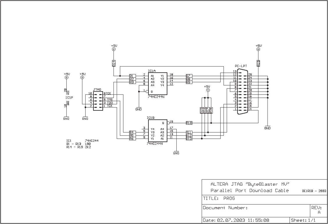
Image 1: JTAG programmer
For this you can either buy a commercially available developer kit for a few hundred euros our you can build your own.
This project uses programable chips from Altera just because they where readily available but there are also others like for example Xilinx.
To start with programmable logic devices just build the programmer cable and the module and download the programmer software from the altera homepage and that's it.
This page is not intended to teach you how to design your chips (ther are numerous other, better ones - see the links at the end of this page)!
DISCLAIMER:
THIS CONTENT IS PROVIDED TO INTERESTED PEOPLE "AS IS" FOR NON COMERCIAL
PURPOSE ONLY. UNDER  NO CIRCUMSTANCES I AM RESPONSIBLE  FOR ANY DAMAGES
TO  YOUR RADIO, PC OR OTHER  EQUIPMENT. THIS  DEVICE  WAS TESTED  UNDER
DIFFERENT  CONDITIONS   AND  UNTIL  NOW  IT  WORKS   WITHOUT  PROBLEMS.
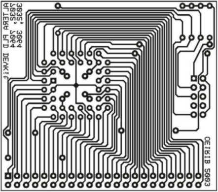
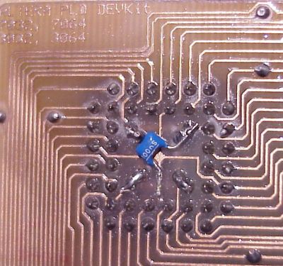
Image 1: The PCB Layout of the FPGA Module
|
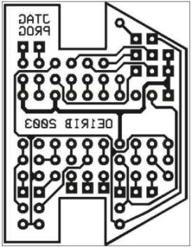
Image 2: The PCB Layout of the JTAG programmer
|
|
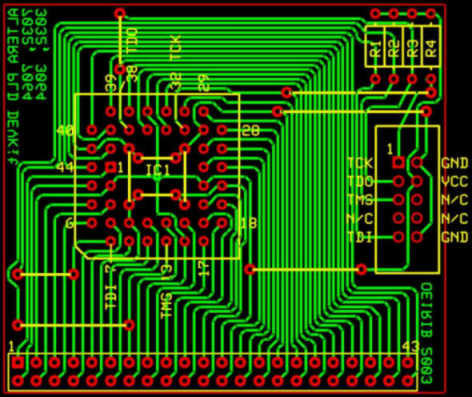
Image 3: Component positions for the FPGA Module
|
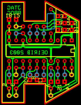
Image 4: Component positions for the JTAG programmer
|
You can download a PDF File with the schematic and the PCB here.
If you
dont have the Adobe Acrobat Reader installed on your machine you can find it here
![]()
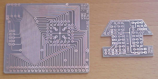
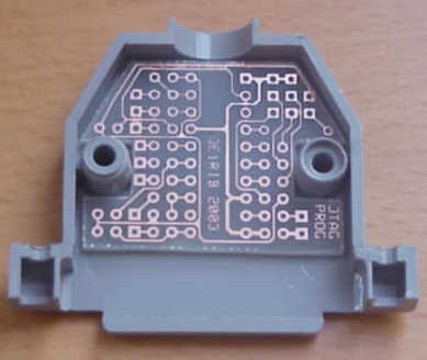
Image 6: The JTAG programmer PCB inside the LPT plug |
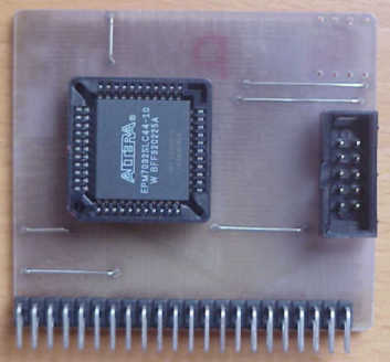
Image 7: The finished FPGA Module |
|
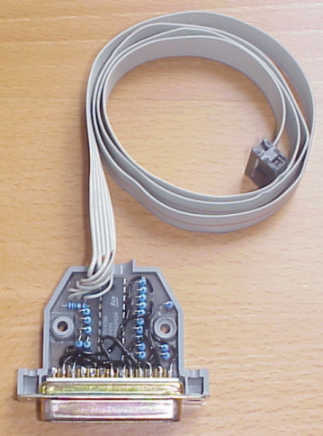
Image 8: The finished JTAG programmer |
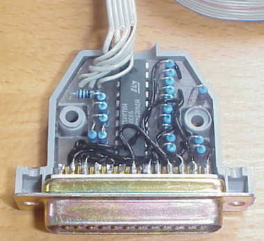
Image 9: A CloseUp of the finished programmer |
 |
This paper can also be found in the german HAM Radio Magazine "Funkamateur" at www.funkamateur.de, Issue 11 / 2003, Page 1090, Title: "Wir bauen uns einen PLD-Chip!" |
73, OE1RIB