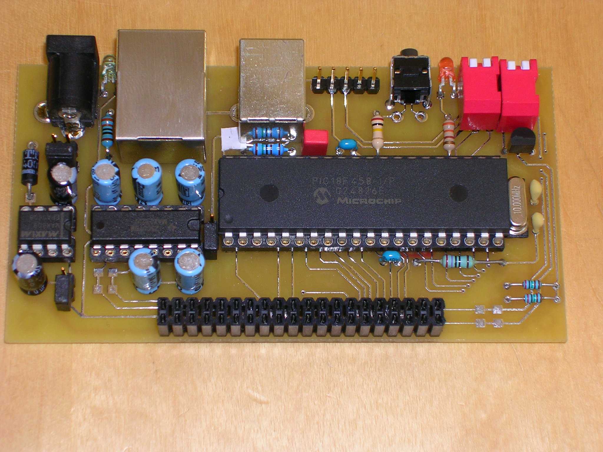
| Jumper |
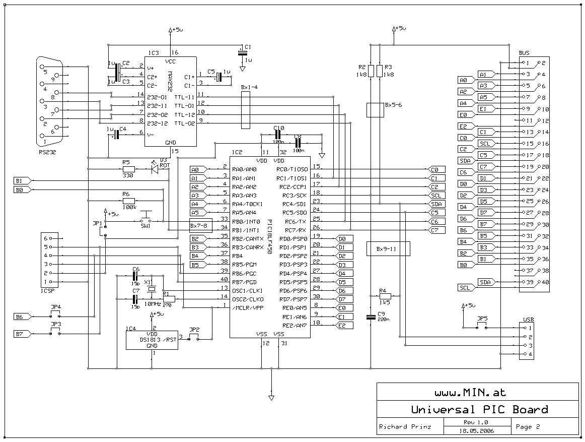
JP1 | DIP-SW | ICSP VDD | |
JP2 | DIP-SW | ICSP MCLR | |
JP3 | DIP-SW | ICSP Port B7 | |
JP4 | DIP-SW | ICSP Port B6 | |
JP5 | Jumper | use USB power | |
JP6 | Jumper | use external power | |
Bx1 | SMT | RS232 CTS on Port C1 | closed |
Bx2 | SMT | RS232 RTS on Port C2 | closed |
Bx3 | SMT | RS232 RX on Port C7 | closed |
Bx4 | SMT | RS232 TX on Port C6 | closed |
Bx5 | SMT | I2C SCL PullUp R2 on VDD | closed |
Bx6 | SMT | I2C SDA PullUp R3 on VDD | closed |
Bx7 | SMT | Switch SW1 on Port B0 | closed |
Bx8 | SMT | LED D3 on Port B1 | closed |
Bx9 | SMT | USB D- on C5 | open |
Bx10 | SMT | USB D+ on Port C4 | open |
Bx11 | SMT | USB PullUp R4 on Port C32 | open |
| |
| Connectors |
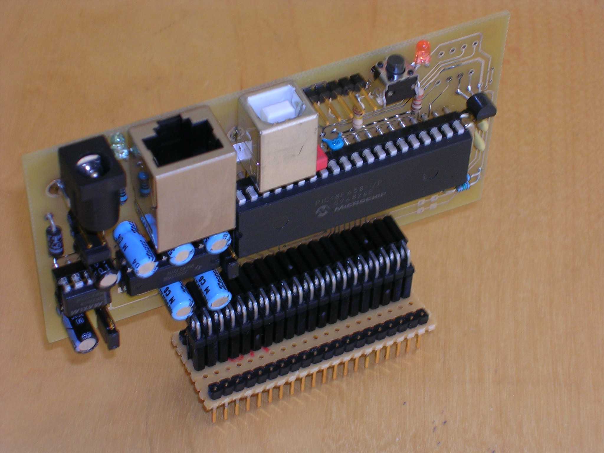
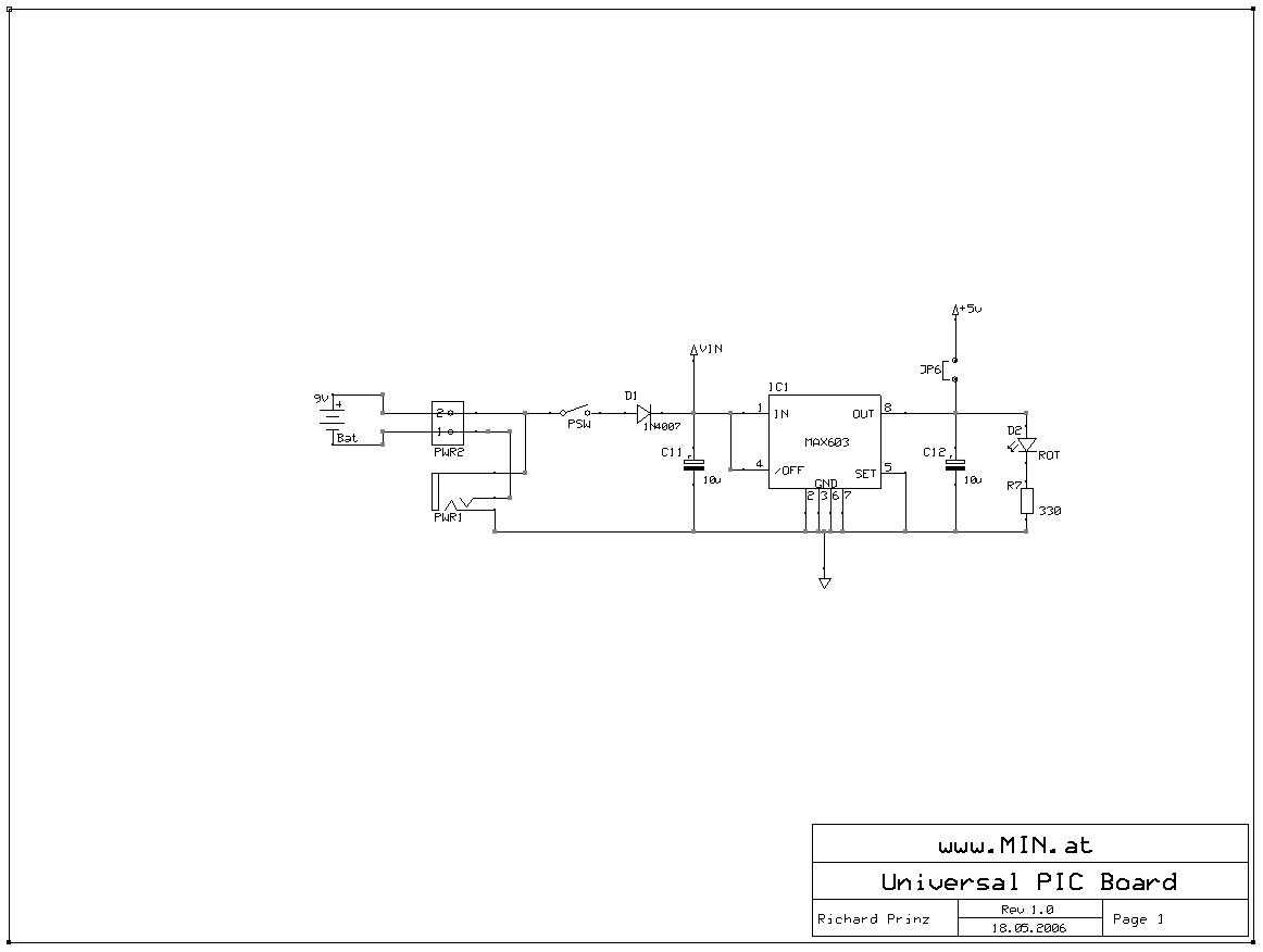
| PWR1 | Barrel | external power supply |
| PWR2 | 2Pin Jumper | Internal power supply (battery).
Disconnected by switch on PWR1 if external power used |
| PSW | 2Pin Jumper | Connector for On/Off switch |
| RS232 | RJ45 | Serial interface (DTE). To connect to a PC use a
1:1 streight cable from RJ45 to SUB-D9. |
| USB | USB-B | USB Connector |
| ICSP | 5 pin SIP | In Circuit Serial Programmin connector (ICSP)
- GND
- VDD
- MCLR
- Port B6
- Port B7
| |
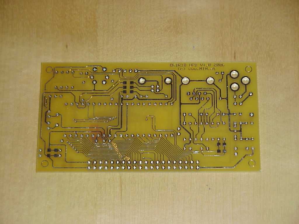
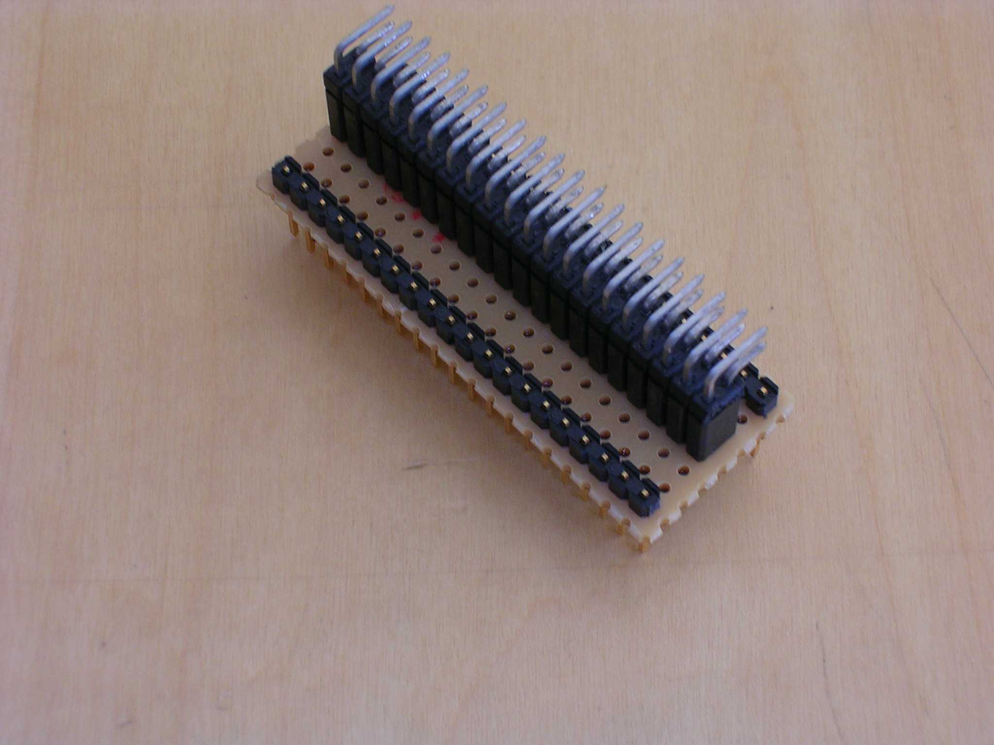
| BUS | 40 pin header | expansion bus
- GND
- VDD
- A1
- A0
- A3
- A2
- A5
- A4
- E1
- E0
- N/C
- E2
- C1 - RS232 CTS
- C0
- C3 - I2C SCL
- C2 - RS232 RTS
- C5
- C4 - I2C SDA
- C7 - RS232 RX
- C6 - RS232 TX
- D1
- D0
- D3
- D2
- D5
- D4
- D7
- D6
- B7
- B6
- B5
- B4
- B3
- B2
- B1
- B0
- N/C
- N/C
- C4 - I2C SDA
- C3 - I2C SCL
| |