Easy SoC Networking - Playing with FPGAs
Tuesday, April 28, 2020
 In my day to day business I work with Software Defined Networking (SDN) a lot. Especially with Open-Flow, Open-vSwitch and some commercial products.
Most of the time the projects are not “normal” ones where these techniques are used in larger scenarios like enterprise or data-center networks. Instead I use them on the other side of the scale in embedded environments for example to develop Space based satellite routers.
At the time of this writing we now have almost eight weeks lock-down due to the SARS-CoV-2 pandemic. This means no travel time to my office and instead working from home. So this spare time must be filled with some experiments. Unfortunately at home I don’t have the resources I normally have at my workplace. So no fancy, multi k-euro development boards and tools. Wanting an embedded system with at least two Ethernet interfaces I looked around in my electronic junkyard and found some interesting components which might give a not so bad platform for some networking experiments. Especially low level Ethernet packet handling (filtering, modifying) is on of my interests. Maybe playing with P4, NetCope, or P4FPGA without spending a fortune.
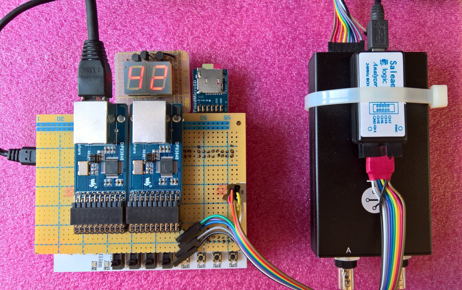
I found the folowing components:
- Digilent Arty-S7-50 development board
- Digilent SD-Card PMOD
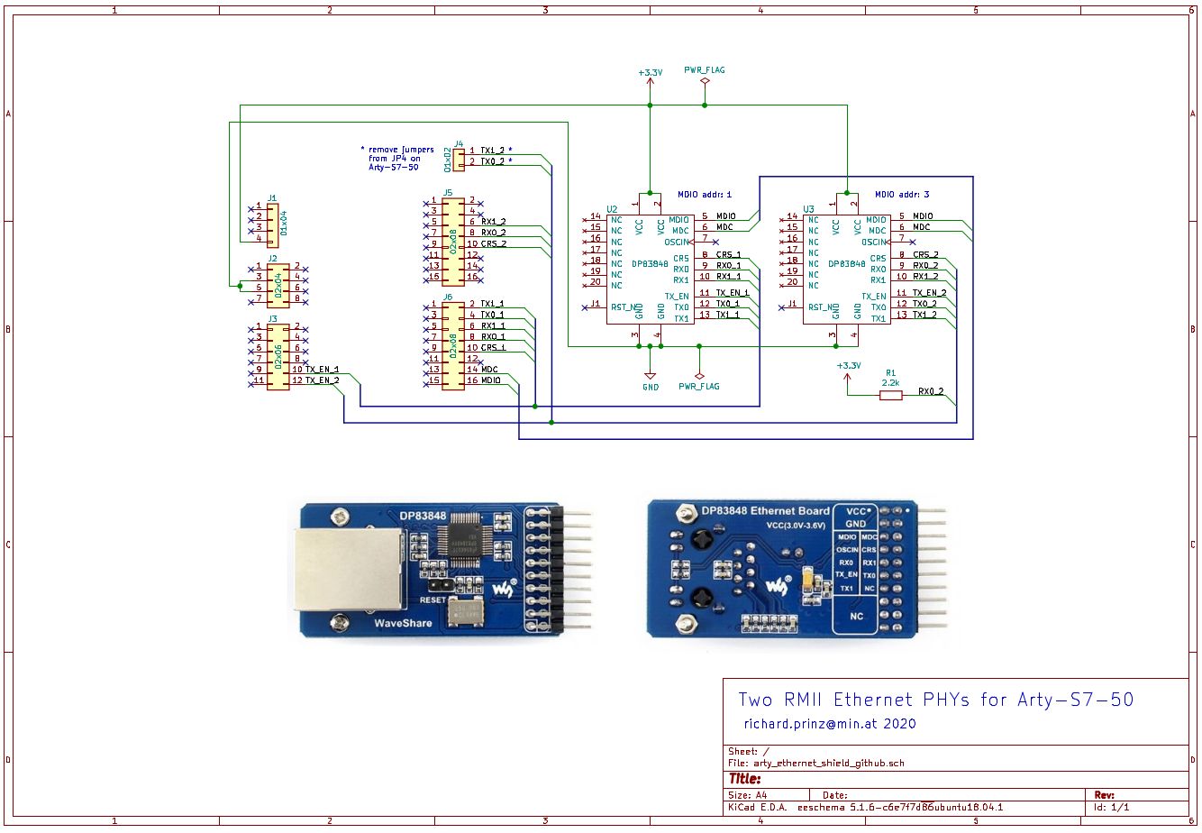
- Waveshare DP83848 Ethernet Phy (2x)
- Two seven segment displays and some resistors and transistors to drive them
The Arty-S7-50 has a not so bad Xilinx Spartan 7 FPGA (XC7S50-1CSGA324C) but unfortunately almost no I/Os. Only four 8-Pin PMODS where only two are usable for digital I/O and the other two are used for analog purposes and a Chipkit/Arduino shield connector which replicates two of the PMODs. So, all in all, compared to other FPGA boards with mezzanine connectors carrying 100dreds of I/Os, not many I/Os to connect peripherals to. Even worse, it has no Ethernet interface(s).
There were also two Texas Instruments DP83848 Ethernet Phy boards from Waveshare lying around. They provide a Reduced Media Independent Interface (RMII) which should match the limited I/Os of the Arty-S7.
A SD-Card PMOD (SPI) used to easily load firmware or boot Linux would also be a nice addition. The Arty-S7 has some buttons, switches and LEDs to interact with but I wanted something a little bit easier to read then LEDs blinking results (Morse …). Two seven segment displays salvaged from an old digital clock, some resistors and transistors provide a simple way to visualize system state without the need for a connected serial console.
The schematic shows how all is connected together. Two pieces of perfboard, one carrying the Ethernet modules and another small one for the seven segment display PMOD are also needed.
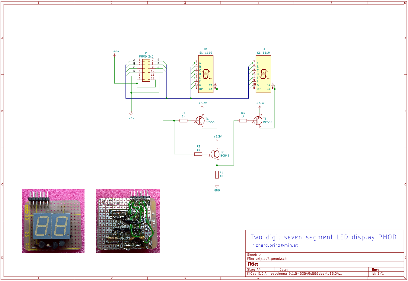
The display PMOD has no support for a decimal point LED instead it uses this signal to multiplex between the two LED displays. This makes it possible to drive two digits from one PMOD multiplexed instead of needing two PMODs like on commercial ones.
Now that everything is built the question arrises how to use the system. At the moment it just has its empty FPGA. As the used FPGA is a Xilinx product you should have installed Vivado (the free version is all you need) to do something usefull with it.
Note: I am not a big fan of vendor Toolchains. They are huge (I mean multi GB) in size and provide Development Environments which need years of practice to master them. But more and more Open-Source Toolchains are appearing recently (e.g. SymbiFlow).
So I had to implement logic for driving the seven segment display, the SD-Card via SPI, Ethernet MACs and at least some logic which glues all that together to do someting usefull e.g. forwarding and filtering packets. Firing up my trusty VIM editor and started to hack together som Verilog. Half way through I decided that it will take too long to come to results. I always wanted to try some alternate HDLs beside the big two VHDL and Verilog.
As Python is one of my main programming languages I was happy to find two Python based HDL languages: MyHDL and Migen. Trying both I’m more comfortable with Migen then with MyHDL. Both generate Verilog (MyHDL also VHDL) based on Python expressions where MyHDL directly uses the Python AST (see also MyHDL and pYosys) whereas Migen implements its own Fragmented Hardware Description Language (FHDL) domain specific language.
Migen besides its FHDL contains a rich set of building blocks for commonly used functions like Finite State Machines (FSM) etc. A really nice feature of Migen is that it can even orchestrate your toolchain. That makes it possible to write a platform description (for the board used), the system description (the application logic) and the build instructions (to configure and run the toolchain) all in Python. No TCL scripting required normally used by vendor tollchains!!
Based on Migen the LiteX SoC builder makes it dead easy to design SoC’s consisting of various CPU cores, buses, memories, interfaces and custom logic. For this little project I choose the VexRiscv core, two MACs to control the Ethernet interfaces and my own seven segment display controller. Later the system will be extended by low level packet inspection in FPGA and a custom firmware loaded from SD-Card.
Unfortunately there was no existing LiteX board description available for the Arty-S7-50. So the first thing was to take its schematic (As there are different board revisions availabe be sure to get the correct one. Mine was the Rev. E) and create one describing its used parts, connections, clocks and toolchain parameters. Its much like a conventional constraints file used in vendor toolchains but somehow smarter. This board information is then instantiated in the main logic which also instantiates the other components like CPU cores, interfaces or custom logic and connectes all these together.
The LiteX build performs the following steps:
- process Migen FHDL (instantiating Modules etc.)
- translate FHDL objects in memory to Verilog
- orchestrate vendor toolchain to produce a FPGA bitstream
- optionally load bitstream info FPGA or into boot flash
During the LiteX build not only the FPGA bitsream is built but also the LiteX BIOS. It is already configured for the correct peripherals enabled in the platform. So if you enabled an SD-Card the BIOS would include the possibility to load binaries from it. Also for enabled Ethernet it would have commands to load binaries via TFTP. See the following console log.
        __   _ __      _  __
       / /  (_) /____ | |/_/
      / /__/ / __/ -_)>  <
     /____/_/\__/\__/_/|_|
   Build your hardware, easily!
 (c) Copyright 2012-2020 Enjoy-Digital
 (c) Copyright 2007-2015 M-Labs
 BIOS built on Apr 28 2020 17:18:55
 BIOS CRC passed (d81bea9a)
 Migen git sha1: --------
 LiteX git sha1: 56aa7897
--=============== SoC ==================--
CPU:       VexRiscv @ 100MHz
ROM:       32KB
SRAM:      4KB
L2:        8KB
MAIN-RAM:  262144KB
--========== Initialization ============--
Ethernet init...
Initializing SDRAM...
SDRAM now under software control
Read leveling:
m0, b0: |00000000000000000000000000000000| delays: -
m0, b1: |00000000000000000000000000000000| delays: -
m0, b2: |00000000000000000000000000000000| delays: -
m0, b3: |00000000000000000000000000000000| delays: -
m0, b4: |00000000000000000000000000000000| delays: -
m0, b5: |00000000000000000000000000000000| delays: -
m0, b6: |00001111111111111000000000000000| delays: 10+-06
m0, b7: |00000000000000000000000000000000| delays: -
best: m0, b6 delays: 10+-06
m1, b0: |00000000000000000000000000000000| delays: -
m1, b1: |00000000000000000000000000000000| delays: -
m1, b2: |00000000000000000000000000000000| delays: -
m1, b3: |00000000000000000000000000000000| delays: -
m1, b4: |00000000000000000000000000000000| delays: -
m1, b5: |10000000000000000000000000000000| delays: 00+-00
m1, b6: |00001111111111111000000000000000| delays: 10+-06
m1, b7: |00000000000000000000000000000000| delays: -
best: m1, b6 delays: 10+-06
SDRAM now under hardware control
Memtest OK
Memspeed Writes: 262Mbps Reads: 327Mbps
--============== Boot ==================--
Booting from serial...
Press Q or ESC to abort boot completely.
sL5DdSMmkekro
Timeout
SD Card via SPI Initialising
SD Card Timeout
Booting from network...
Local IP : 192.168.1.50
Remote IP: 192.168.1.100
Fetching from: UDP/69
Unable to download boot.bin over TFTP
Network boot failed
No boot medium found
--============= Console ================--
litex> help
LiteX BIOS, available commands:
mr         - read address space
mw         - write address space
mc         - copy address space
mdiow      - write MDIO register
mdior      - read MDIO register
mdiod      - dump MDIO registers
crc        - compute CRC32 of a part of the address space
ident      - display identifier
flush_cpu_dcache - flush CPU data cache
flush_l2_cache   - flush L2 cache
reboot     - reset processor
netboot    - boot via TFTP
serialboot - boot via SFL
memtest    - run a memory test
spisdcardboot   - boot from SDCard via SPI hardware bitbang
litex>
litex>
litex> ident
Ident: Arty-S7 RISC64 v1.0 2020-04-28 17:18:50
litex>
To interface custom logic in FPGA with higher level code running on the embeded CPU, LiteX/Migen uses the concept of Configuration and Status Registers (CSR). There are three types of such status registers: CSRConstant for constant values, CSRStatus for providing information to the CPU and CSRStorage for allowing control via the CPU. For more infos see the guithub code. In this little system my two logic blocks (the seven segment display and a simple hello-world extension which justs xor’s everythin provided with 0xff as an example) are accessible via these autogenerated CSR’s from application logic. Same is true for the high level access to the Ethernet interfaces. Simply include the build/software/include/generated/csr.h in your application and use the provided functions in it.
Code and build instructions can be found Github.